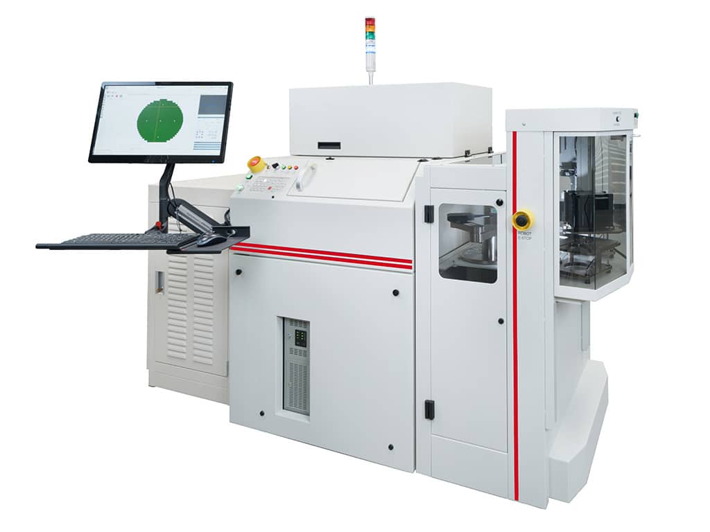
M350 is an advanced platform for high precision, high throughput wafer-level optimization of linear and mixed-signal IC devices.

Beam Positioning |
High-speed closed loop galvanometer scanner |
XY Stage Resolution: | 0.02 μm |
XY Stage Accuracy: | ± 2.0 μm |
Wafer Size: | Supports 100 – 200 mm wafers |
Stage: | X, Y, Z, W, Theta |
Spot size: | 6.5 μm to 12 μm (optional 5 μm) |
Part loading: | automated (manual as option) |
User friendly WaferTrim™ software improves efficiency and provides compatibility with existing M310 data setup files
Exclusive license rights to the wafer trim product range of Electro Scientific Industries, Inc. (ESI)
With the license agreement, the Photonics Systems Group, and with this L-TRIS, receives access to patents and know-how for the production, support and service of the ESI M350 wafer trim system. The goal of the agreement is to ensure worldwide service and support for ESI’s existing wafer trim customers and to further develop the product market for the companies of the group.
Haben Sie Fragen zu unseren Produkten und Services?